
Norcott installs 3D solder paste inspection system
Norcott has installed three-dimensional solder paste inspection equipment in Cheshire. The Koh Young KY8030-2 measures deposit height, area, and volume before component placement, providing data to refine stencil design, printer settings, and production quality controls.
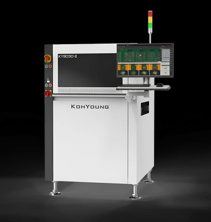
Norcott Technologies has installed a Koh Young KY8030-2 three-dimensional solder paste inspection system at its Cheshire electronics manufacturing facility, introducing additional measurement capability before components are placed onto printed circuit boards.
Supplied through Altus Group, the equipment is already providing information used to evaluate stencil designs and optimise solder paste printing programmes. The investment follows a review of Norcott's surface mount assembly operations, with greater emphasis on detecting printing variations before they affect subsequent manufacturing stages.
The manufacturer identified solder paste inspection as an investment priority during 2025. It wanted to strengthen process control and improve first-pass yield by obtaining more detailed measurements of the material deposited onto printed circuit boards.
Solder paste printing is one of the first operations in surface mount technology assembly. A stencil is positioned over a circuit board, allowing paste to be deposited through precisely formed apertures onto the pads where electronic components will subsequently be mounted.
The printed board then passes through component placement and reflow soldering, during which controlled heating melts the solder and forms electrical and mechanical connections between the components and the board.
Variations introduced during printing can affect the quality of those connections. Insufficient solder paste may result in incomplete joints, while excessive material or deposits extending outside the intended area can increase the likelihood of bridging between adjacent contacts.
The geometry of a solder deposit is particularly important when manufacturing assemblies containing fine-pitch components. Closely spaced pads leave limited room for variation, and faults introduced during printing may be difficult to inspect once components have been placed.
Measuring the deposits before placement provides an opportunity to identify a process problem while the board remains accessible. The inspection result can then be used to determine whether a board should proceed or whether the printing operation requires attention.
The KY8030-2 uses three-dimensional measurement technology to determine the height, area, and volume of individual solder paste deposits. These measurements provide more information than a two-dimensional image showing the deposit's apparent position and outline.
Deposit volume is especially useful because a printed feature can appear correctly positioned while containing too much or too little material. Comparing measured volume with defined process limits allows engineers to identify departures from the intended printing result.
The system employs dual-projection Moiré technology to reconstruct the surface profile of deposited paste. Projected patterns are analysed to determine variations in height across the measured region, enabling the inspection software to calculate three-dimensional characteristics.
Using two projection directions helps address measurement difficulties created by shadows and reflections. These effects can be significant when inspecting small deposits on surfaces containing metallic pads, solder paste, and other materials with different optical characteristics.
Board flatness introduces another potential source of error. Printed circuit boards may be warped or vary slightly in height across their surface, changing the apparent position of deposits relative to a fixed measurement reference.
The KY8030-2 incorporates active warp compensation to detect and account for these variations. This allows inspection results to reflect the actual solder paste geometry more accurately, rather than treating every change in board height as a printing defect.
The resulting measurements can be examined across individual boards and repeated production batches. Patterns in the data may indicate changes in paste transfer, stencil condition, printer alignment, or another part of the printing process.
A consistent reduction in volume across several apertures, for example, would require a different investigation from an isolated deposit extending outside its intended position. The additional measurement detail helps engineers identify where corrective work should be directed.
Stencil design is one area Norcott is already examining using the new information. Aperture dimensions and geometry influence the amount of solder paste transferred to the board, particularly where components require very small or closely spaced deposits.
Changes to printer programmes can also be assessed against measured results. Rather than relying only on subsequent assembly defects to establish whether a setting was effective, engineers can compare deposit measurements before and after a process adjustment.
The inspection system therefore supports process optimisation as well as defect detection. Monitoring changes in measured deposit characteristics provides a basis for investigating process stability and determining whether production adjustments are delivering the intended result.
Norcott assessed available inspection technologies at Productronica in Munich before selecting the equipment. An initial Koh Young demonstration was followed by detailed technical discussions, sample validation, and practical demonstrations arranged with Altus in the UK.
Those evaluations allowed the manufacturer to examine how the system performed against its own assembly requirements before committing to the installation.
Pete Lomas, managing director of Norcott Technologies, said: “Accurate solder paste deposition is fundamental to the performance of an SMT line.”
Altus supported the selection, installation, and introduction of the system into production. The implementation included technical validation and training, enabling Norcott's engineers to begin using the equipment and reviewing measurement data.
The KY8030-2 platform offers additional process control capabilities, including integration with Koh Young's analysis software and an optional solder paste rework module. However, Norcott has not confirmed that every optional feature has been installed or activated.
The initial investment is centred on collecting accurate inspection data and using it to improve the existing printing process. The company has not published a quantified reduction in defects, an increase in first-pass yield, or a measured saving in production time.
Those outcomes would depend on how inspection findings are incorporated into operating procedures and how subsequent process changes affect completed assemblies.
The installation gives Norcott an additional measurement stage before component placement, allowing solder paste quality to be assessed while the deposits remain accessible. Its ongoing use will support decisions on stencil geometry, printer programming, and the stability of the surface mount assembly process.
Written by
People First